
| 2017— |
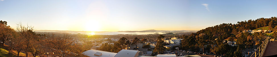
Lawrence Berkeley National Laboratory, Berkeley, CA - USA X-ray Optics research scientist I am designing and simulating the four feature beamlines of the upgrade of the Advanced Light Source, which will leverage the improved performances of the facility. Owing to the extereme precision of the optics, the specifications are extremely tight and require excellent collaboration with engineers and beamline scientists to deliver world-class synchrotron beamlines. | |
| 2017— |
Lawrence Berkeley National Laboratory, Berkeley, CA - USA Advanced x-ray optics project scientist I'm working on ALS-U, the DLSR upgrade of the ALS, where the goal is to produce diffraction-limited soft X-ray beams by pushing physics to the extreme. My main role is to design and study wavefront sensors and adaptive optics for the x-ray range, through simulations and experiments, working hand-in-hand with all the scientists and engineers to solve the many challenges regarding vacuum environment, vibrations and manufacturing tolerances. | |
| 2012-2016 |
Lawrence Berkeley National Laboratory, Berkeley, CA - USA Postdoctoral fellow I've worked at the Center for X-Ray Optics, on x-ray microscopy within the SHARP EUV Microscope team, where we study nanometer scale defects on extreme-ultraviolet photo-masks,for customers such as Intel, IBM or Samsung. My main area of research novel imaging techniques and imaging processing based on illumination diversity, and metroology. I've also worked on the next generation microexposure tool (MET5), on prototyping, tolerancing and qualification of sub-elements, but also software architecture and stage controls. | |
| 2008-2012 |
Lab for Optics & Biosciences (Ecole Polytechnique - CNRS - INSERM), Palaiseau - France Ph.D. in Optics I've worked on terahertz radiations, in order to probe biologicial sample with far-infrared, ultra-short pulses, developping imaging techniques based on the manipulation of polarization and evanescent waves for the study of ion transport in neurons. My PhD dissertation is entitled "Polarization of terahertz waves in the subsingle-cycle regime and application to imaging in biology" |
|
| 2008-2011 |
Universitķ Paris-Sud, Orsay - France Assistant lecturer Teachings in Digital Signal Processing at graduate level (PolytechÆParis-Sud Opto-electronics division). Labclasses in Optics and DSP at Universitķ Paris-Sud, and THz science experimental activities at ╔cole Polytechnique |
|
| 2008 | Thales Technology Center Singapore, Singapore Engineering intern IÆve worked on the design and the prototyping of a high-speed, free-space optical communication scheme for commercial use in aircrafts. The solution makes use of computer-generated holograms, fiber optics and advanced modulation schemes (OFDM). | |
| 2007 |
Valtionen Teknillinen Tutkimuskeskus (VTT) - Technological Center of Finland, Oulu - Finland Research intern IÆve worked on the nano-imprinting process of subwavelength anti-reflective structures, alongside with the determination of physical properties of thin-film solar cells (CIGS). |
|
| 2006 | smart S.A.S. France, Hambach - France. Regular worker I've worked as a regular worker on the assembly line, mainly mounting headlights on the 2-seated cars. |
| 2008-2012 |
╔cole Polytechnique, Lab for Optics & Biosciences, Palaiseau - France Ph.D. in Optics - summa cum laude Top French engineering school and research center. | |
| 2005-2008 | ╔cole Centrale de Marseille, Marseille - France Master's Degree in engineering Major : Optics and Photonics. Complementary courses in medical imaging. |
|
| 2008 | Universitķ Aix-Marseille, Marseille - France M.Sc. in Optics and Image Processing - magna cum laude Major : Optics and Electromagnetism |
|
| 2003-2005 | Lycķe Klķber, Strasbourg - France Preparatory classroom MPSI/MP |
|
| 2003 | Lycķe de Iles du Nord, Saint-Martin (French West Indies) Baccalaurķat scientique - first class honors (mention TB) |
I grew up on the islands of Guadeloupe and Saint Martin, in the French West Indies, since the age of 9.
"Physics of femtosecond pulses" CNRS Workshop in Les Houches (France) (1 week)
"Negotiation and Management" doctoral school seminaries (2 weeks)
"Research valorization through the creation of start-ups" residential seminary (1 week)
"Creation of Start-ups" ╔cole Polytechnique course (40h+)
Spoken languages
|
Programming languagesMatlab, python, Julia, C#Windows, MacOS, Linux Matlab, Zemax (adv. knowledge), Labview Code V, Meep Word, Excel, Powerpoint, Latex, etc. |
| General: science, literature, philosophy, epistemology, DIY electronics (Arduino), photography |
| Sports: bouldering, biking, windsurf, sailing (resume, quite old!) |
| Associations: Berkeley Lab Postdoc Association, Berkeley Entrepreneurship Program, Massilia Dķfi Voile, XÆDoc, SPIE Student Chapter |
ōDirect patterning of micro-optical structures by combined nanoimprinting
and lithographyö
Jarkko Tuominen, Jussi Hiltunen, A. Wojdyla et al. in Proceedings of SPIE 69920B-69920B-8 (2008) — pdf
ōBeam waist measurement for terahertz time-domain spectroscopy experimentsö
A Podzorov, A Wojdyla, G. Gallot in Optics Letters 35, 7, 901-903 (2010) —pdf
ōBrewster’s angle silicon wafer terahertz linear polarizerö
A Wojdyla, G Gallot, in Optics Express 19,15, pp. 14099-14107 (2011) — pdf
ōTotal Internal Reflection Terahertz Imagingö
A Wojdyla, G Gallot in Proc. 36th IRMMW-THz Conference (2011) —pdf
ōAchromatic polarizing elements for pulsed THz wavesö
A Wojdyla, G Gallot in Proc. 36th IRMMW-THz Conference (2011) — pdf
ōAttenuated Internal Reflection Terahertz Imagingö
A Wojdyla, G Gallot in Optics Letters 38, 2, pp. 112-114 (2013) —pdf
ōPhase noise investigation in terahertz time-domain spectroscopy measurementsö
A Wojdyla, G Gallot, IRMMW-THz Conference (2013) — pdf — extended draft
ōSpectral phase, temporal phase and carrier-enveloppe phase of sub-single cycle terahertz pulsesö
A Wojdyla, G Gallot, in preparation (2012)
ōPtychographic wavefront sensor for high-NA EUV inspection and exposure toolsö
A Wojdyla, R Miyakawa, P Naulleau in Proc. SPIE Extreme Ultraviolet Lithography V, 904839 (2014) — pdf
ōCoded aperture detector : an image sensor with sub 20-nm pixel resolutionö
R Miyakawa, R Mayer, A Wojdyla et al. in Optics Express 22, 16 (2014) — draft
ōActinic mask imaging: recent results and future directions from the SHARP EUV microscopeö
K G Goldberg, M P Benk, A Wojdyla et al. in Proc. SPIE Extreme Ultraviolet Lithography V, 90480Y (2014) — pdf
ōA broader view on EUV-masks: adding complementary imaging modes to the SHARP microscopeö
M P Benk, R Miyakawa, W Chao, Y Wang A. Wojdyla et al. in Journal of Micro/Nanolithography, MEMS, and MOEMS 14, 1 (2015)
ōAberration estimation using EUV mask roughnessö
R A Claus, A Wojdyla, M P Benk, K A Goldberg, A R Neureuther, P P Naulleau, L Waller
in Proc. SPIE 9422, Extreme Ultraviolet (EUV) Lithography VI, 942214 (2015)
ōA method of image-based aberration metrology for EUVL toolsō
Z Levinson, S Raghunathan, E Verduijn, O Wood, P Mangat, K Goldberg, M Benk, A Wojdyla, V Philipsen, E Hendrickx, B W Smith in Proc. SPIE 9422, Extreme Ultraviolet (EUV) Lithography VI, 942215 (2015)
ōNew ways of looking at masks with the SHARP EUV microscopeö
K A Goldberg ; M P Benk ; A Wojdyla et al. in Proc. SPIE 9422, Extreme Ultraviolet (EUV) Lithography VI, 94221A (2015)
ōEnhancing defect detection with Zernike phase contrast in EUV multilayer blank inspectionö
Y Wang ; R Miyakawa ; W Chao ; M Benk ; Antoine Wojdyla et al.
Proc. SPIE 9422, Extreme Ultraviolet (EUV) Lithography VI, 94221C (2015)
ōMask blank defect printability comparison using optical and SEM mask and wafer inspection and bright field actinic mask imagingö
P Mangat, E Verduijn, O R Wood, M P Benk, A Wojdyla, K A Goldberg
in Proc. SPIE 9658, Photomask Japan 2015: Photomask and Next-Generation Lithography Mask Technology XXII
pdf
ōFourier Ptychography Microscopy for increased spatial resolution at extreme ultraviolet wavelengths using an angle-scanning illuminatorö
A. Wojdyla, M. P. Benk, D. J. Johnson, A. Donoghue, K. A. Goldberg, in preparation_(2015)
ōEUV actinic brightfield mask microscopy for predicting printed defect imagesö
K A Goldberg, M P Benk, A Wojdyla et al. in Proc. SPIE 9635, 963514 (2015)
ōExamination of phase retrieval algorithms for patterned EUV mask metrologyö
R A Claus, Y-G Wang, A Wojdyla et al. in Proc. SPIE 9635, 96350F, (2015)
ōMask blank defect printability comparison using optical and SEM mask and wafer inspection and bright field actinic mask imagingö
P Mangat, E Verduijn, Obert R. Wood II, et al. in Proc. SPIE 9658, 96580E (2015)
ōAssessment of AIMS EUV and SHARP actinic wavelength mask defect review tools for the evaluation of blank defect printabilityö
E Verduijn, E Hosler, P Mangat, O Wood et al. in 2015 International Symposium on EUV Lithography
ōUsing the SHARP EUV Microscope's aerial images to study line edge roughnessö
A Wojdyla, A Donoghue et al. in 2015 International Symposium on EUV Lithography
ōDemonstration of 22-nm half pitch resolution on the SHARP EUV microscopeö
M P Benk, K A Goldberg, A Wojdyla et al. in Journal of Vacuum Science and Technology B 33 (6), 06FE01 (2015)
ōActinic mask imaging: Taking a SHARP look at next generation photomasksö
M P Benk, A Wojdyla, K A Goldberg, Patrick Naulleau in 2015 International Symposium on EUV Lithography
ōEmulation of anamorphic imaging on the SHARP extreme ultraviolet mask microscopeö
M P Benk, A Wojdyla et al. in J. Micro/Nanolith. MEMS MOEMS 15(3), 033501 (2016) (pdf)
ōMeasurement of EUV lithography pupil amplitude and phase variation via image-based methodologyö,
Z Levinson, E Verduijn, O R Wood, P Mangat, K A Goldberg, M P Benk, A Wojdyla and B W Smith in
J. Micro/Nanolith. MEMS MOEMS 15(2), 023508 (2016) (pdf)
ōUltrahigh efficiency EUV contact - hole printing with chromeless phase shift maskö,
P Naulleau, C N Anderson, W Chao, K A Goldberg, E Gullikson, F Salmassi, A Wojdyla in Proc. SPIE 99840P (2016)
(pdf)
ōAerial imaging study of the mask-induced line-width roughness of EUV lithography masksö
A Wojdyla, A Donoghue,M P Benk, P P Naulleau and K A Goldberg in SPIE 97760H, (2016)
(pdf)
ōOff-axis aberration estimation in an EUV microscope using natural speckleö
A Shanker, A Wojdyla et al. in 2016 Imaging and Applied Optics Congress ITh1F.2
(pdf)
ōAmplitude versus phase effects in extreme ultraviolet lithography mask scattering and imagingö
P Naulleau, M Benk, K Goldberg, E Gullikson, A Wojdyla, YG Wang, and A Neureuther
Reviewer for Optics Letter, Optics Express
European Optical Society Annual Meeting – Paris, France (October 2010)
6th Terahertz Days – La Grande-Motte, France (May 2011)
Infrared, Millimeter Waves and Terahertz Conference (IRMMW) – Houston, TX, USA (October 2011)
SPIE Extreme Ultraviolet Lithography – San Jose, CA, USA (February 2014)
SPIE Photomask Technology 2014 (SPIE/BACUS) – Monterey, CA, USA (September 2014)
EUVL Symposium 2014 – Washington, DC, USA (October 2014)
SPIE Extreme Ultraviolet Lithography – San Jose, CA, USA (February 2015)
SPIE Photomask Technology 2015 (SPIE/BACUS) – Monterey, CA, USA (September 2015)
SPIE Extreme Ultraviolet Lithography – San Jose, CA, USA (February 2016)
SPIE Photomask Technology 2016 (SPIE/BACUS) – Berkeley, CA, USA (September 2016)
Photon Diag 2017 – Menlo Park, CA, USA (May 2017)