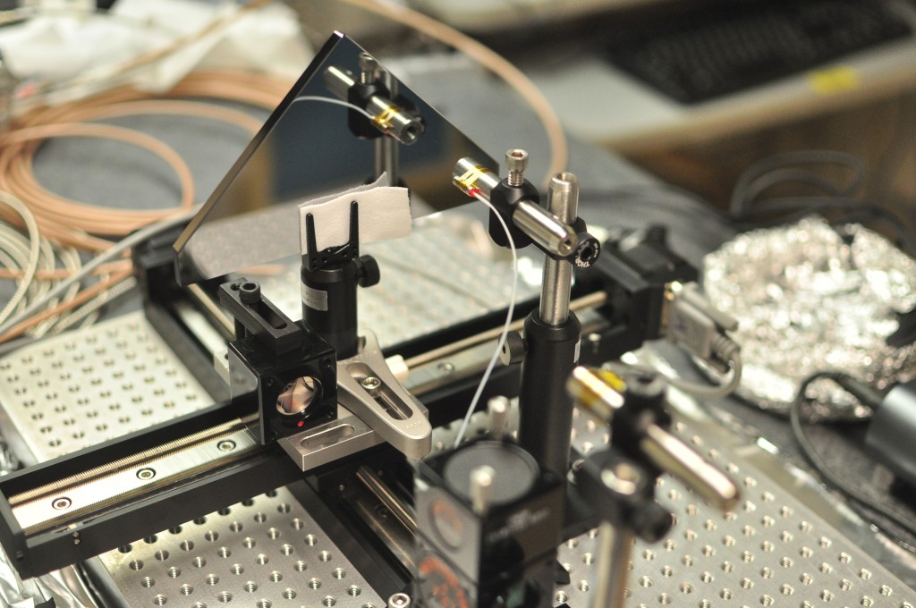
Over the past four years, I’ve been working on two of the EUV tools at the Center for X-Ray Optics, and while I’m moving to new projects, it’s time I give some explanations about what these two projects are about, the SHARP EUV microscope, and the 0.5NA Micro-Exposure Tool (MET5.)
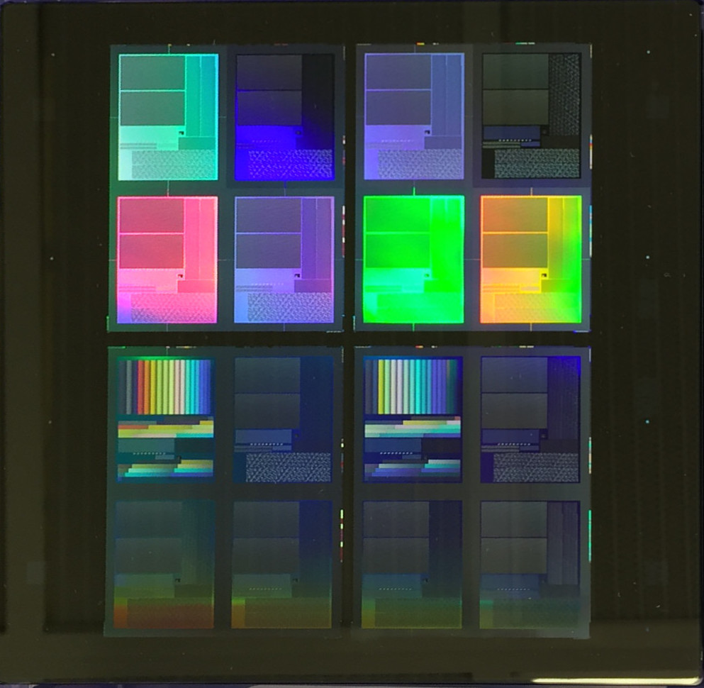
SHARP (sharp.lbl.gov) is the Sharp High-NA Actinic Recticle review Project, a (very) soft x-ray full-field microscope designed to record images of EUV photomasks.
- EUV: Extreme Ultraviolet, a range wavelength between soft X-Rays and Vacuum Ultraviolet, which is poised to be the next generation in semiconductor manufacturing technology.
- Actinic (aka “at-wavelength”, λ=13.5nm): we are looking at things as they are in a lithography stepper
- Reticle (aka photomasks): we are looking at the gold-master (the “mold”) of the electronic circuits that will be printed on every chip that will be printed in the semiconductor foundry.
- Review (aka inspection): we are specifically looking at defects on these photomasks, for the would print on all the latter mentioned chip, dramatically decreasing the yield of the factory.
- High-NA (high numerical aperture): the resolution of our tool is as close as possible to what is physically allowed (the diffraction limit.)
It is designed to emulate EUV lithography steppers, such as ASML NXE3300.
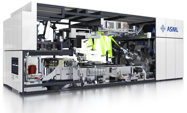
ASML NXE:3300 EUV stepper, with 0.33NA optics
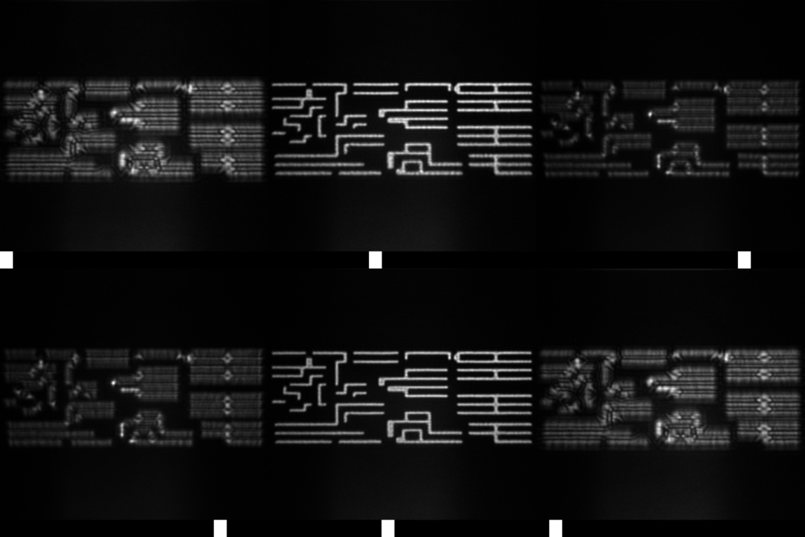
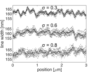
Contrary to most x-ray microscope, SHARP is a “full-field” microscope, meaning that it actually creates an image of the object on the camera, while most x-ray microscopes are either scanning microscopes (STXM), where a tiny spot is swept across the sample to image it point by point, or coherent diffraction images, where there is no optics, and the sample is reconstructed numerically after some computations. In addition, it features a Fourier coherence synthesizer, which allows to tailor the illumination of the sample in order to mimic modern steppers and explore tricks to improve the resolution.
The main goal of this tool is to image defects on EUV masks, often caused but tiny (<5nm) imperfection.
The typical resolution is 50 nm, corresponding to wafer-side dimensions of 13nm, taking into account the 4x de-magnification factor of EUV printers.
I’ve been operating this tool for two years, working on a daily basis with company such as Intel, Global Foundries or Samsung. I was mostly interested in keeping the tool running, improving it from time to time (e.g. adding interferometer heads to improve positioning accuracy), and the development of new techniques for characterization of the tool or the mask under study.
It is quite fun to measure things in photon per square nanometers:)
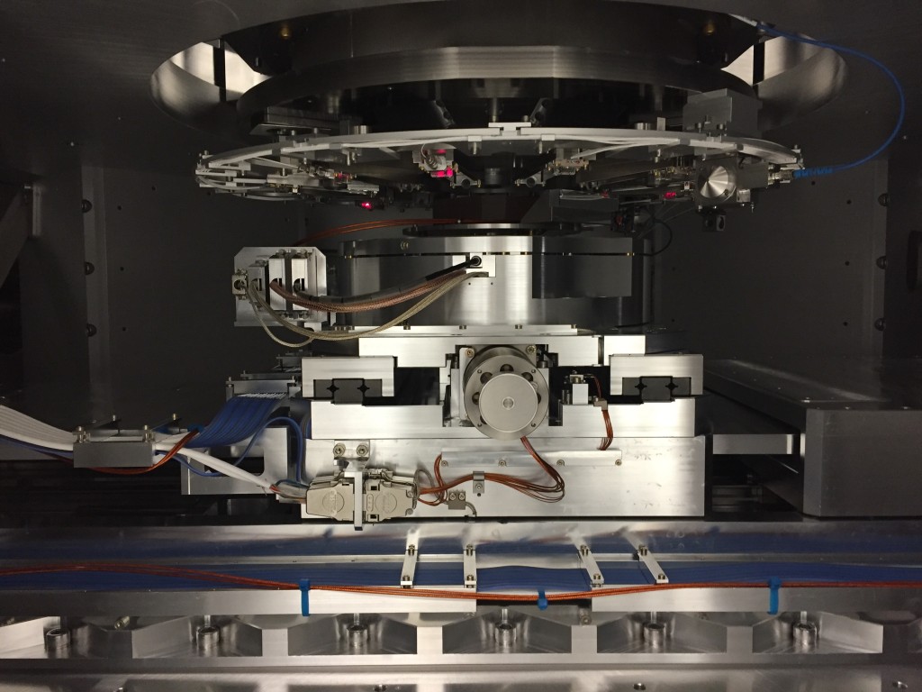
MET5 is the first project I was working on, and it now nearing completion. It is a research-grade EUV lithography printer (Micro-Exposure Tool) that has a 0.5NA optics, larger than all those available in current printing EUV tools. Its ultimate resolution is 8nm. In order to achieve this, it is equipped with a pair of mirrors which ranks among the finest and most expensive ever made, and many, many sensors to compensate for vibration, position error and thermal drift: ensuring less than 1nm drift over exposure time (~1s) for a machine that large is no easy task.[picture]
This project was initially meant to be completed by the end of 2014, but the collapse of the Sematech consortium (apparently caused by shady practices) pushed back the project, which is now slated to start operation at the end of 2017. While this is a terrible waste of time for the wrong reasons, it will still be among the most precise optical nano-fabrication tools ever made.
While EUV stills hasn’t reached microchips foundries, after more than 30 years of development (In his book 1994 “Only the paranoid survives“, Intel’s CEO Andy Grove was already mentioning x-ray lithography), recent progress in source power and lower defective in EUV mask blanks are now pushing the technology forward, and it is now likely that by 2020 your telephone will have a chip printed with this technology.
