I don’t know how to do this on a small scale in a practical way, but I do know that computing machines are very large; they fill rooms. Why can’t we make them very small, make them of little wires, little elements – and by little, I mean little. For instance, the wires should be 10 or 100 atoms in diameter, and the circuits should be a few thousand angstroms across.
– Richard Feynman (1959)
Being a researcher, all my friends and family have very little idea of what I’m work on. The trouble is that when I try to explain, I need to resort to notions such as wavelength or transistor, only to discover that most people have no clue of what this is, expect to joke about being on the same… wavelength. But very small wavelength.
To put it straight : I look at small things.Yet, I was just awarded a prize for best research at the EUV lithography symposium in Washington, D.C., and it’s only fair of me to explain what I’m doing for a living!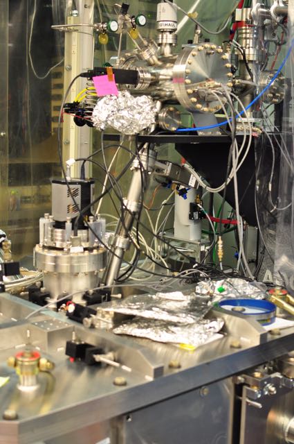
The SHARP EUV microscope I’m working with
I am working at the Center for X-Ray Optics, in a team specialized in EUV lithography. For a starter, let’s explain what this is !
EUV Lithography
(Photo-)lithography is the art of making microchips. As complicated as they might be (they now feature billions of transistor), fabricating microchips is not from photography.
It all starts with a silicon wafer, which is somehow just a piece of highly purified and melt send that has the cool property of being a semi-conductor. The wafer is then coated with what is called a photoresist, which is a sort of resin that gets harder when lit with ultra-violet light. Using this cool property, one can “print” any kind of pattern on the wafer. This is done using a photo-lithography tool (which is a fancy inverted microscope) and a photo-mask (the equivalent for vinyls would be a goldmaster, though in this case it is pressed against the product), whose image will be replicated on the photoresist. The resist is then chemically processed, in order to leave polymer where it was exposed, and nothing everywhere else.Then the wafer can be bombarded with ions to alter its electrical properties-this is called doping-, or some metal can be deposited, the photo-resist left being here to locally prevent these changes, forming some kind of an electrical circuit (well, it’s way more complicated than that, but you get the idea).Repeating this process with different patterns and doping, one can fabricate very complicated electrical functions and finally get a working microchip.*
* *
 As you try to fabricate smaller and smaller feature to satisfy the Moore’s law, you need to have smaller and smaller wavelength. Current photo-lithography tool are using deep ultra-violet light to expose the wafers, with a wavelength of 193 nm. However, they are now printing features that are about 50 nm in dimension. The industry was able to keep using the same wavelength for a while by using immersion lithography and multi-patterning, but the options are becoming more and more limited.That’s where my work comes into play. To keep up with the pace of progress, the principal solution is to change the wavelength to 13.5nm, in the extreme ultra-violet range (EUV).
Many new issues arises : dimensions are so small that everything becomes a disturbance : temperature, vibration, or even the granularity of matter. (I’ve made a presentation for public outreach, available here)My work is focused on the inspection of EUV photo-mask, which is one of the main issues for EUV lithography : a single defect on a mask end up printed on every wafer going out of the fab. That’s why we need new techniques to spot them (they’re as small as a few microns) to be able to repair them.
The SHARP EUV Microscope
I am working in the SHARP team. SHARP stands for
“SEMATECH High-NA Actinic review project” where :
- SEMATECH is the consortium of semiconductors companies (among which Intel, IBM, Samsung, GLOBALFOUNDRIES) that funds us .
- Actinic stands for “at-wavelength”.
- High-NA means “high-resolution”
- review means “inspection of photo-mask”
All in all, it is a fancy synchrotron-based microscope designed to emulate current EUV photo-lithography tools. It features reflective optics coated with silicon-molybdenum multi-layers and diffractive optics to achieve resolutions down to 30 nm (that is 6nm on the wafer side) with custom illumination conditions.
I spend most of my week at the beamline in order to collect data for customers, and I am working on various projects, in order first to improve the stability and the reliability of the system, but also to extend its possibilities.Fourier Ptychography Microscopy
One of my hottest research topics nowadays is Fourier Ptychograhpy Microscopy, which is an recent imaging technique that allows you to improve the resolution of an image significantly and also get 3D information of your sample, by using simple yet powerful tricks in the data acquisition
The term ptychography comes from the greek root ptycho-, which means “to fold”. Originally, ptychography was just a fancy name for a clever improvement of coherent diffraction imaging.The idea of coherent diffraction imaging is to shine a coherent source (a laser, a synchrotron or even LED, with some limitation) on a object, which will then “smear out” the light, which is then collected. The recorded image just look like nothing, but by virtue of the laws of physics, it is possible to reconstruct what was the original object by computationally solving what is called “the phase retrieval problem”. This problem is generally hard to solve accurately, and some researchers devised a clever trick, that is to scan the object, collect the light for all position, and use these different measurements to reinforce the data. There is obviously some overlap in the information contained.Fourier ptychography is just that, except that instead of scanning the object spatially, it is the (coherent) illumination that is scanned angularly, while the setup included an imaging element.The collected data is then crunched using an iterative algorithm that spits out the complex-valued angular spectrum (from an information standpoint, ptychography and Fourier ~ are equivalent), which in turns yield improved resolution and quantitative phase information.(I’ll put images as soon as the corresponding article is be published:)Knowing the phase is of primary importance in photo-mask inspection, because phase defects are the most common defects yet the hardest to spot, since they are often invisible at best-focus. That’s probably what people liked at the conference:)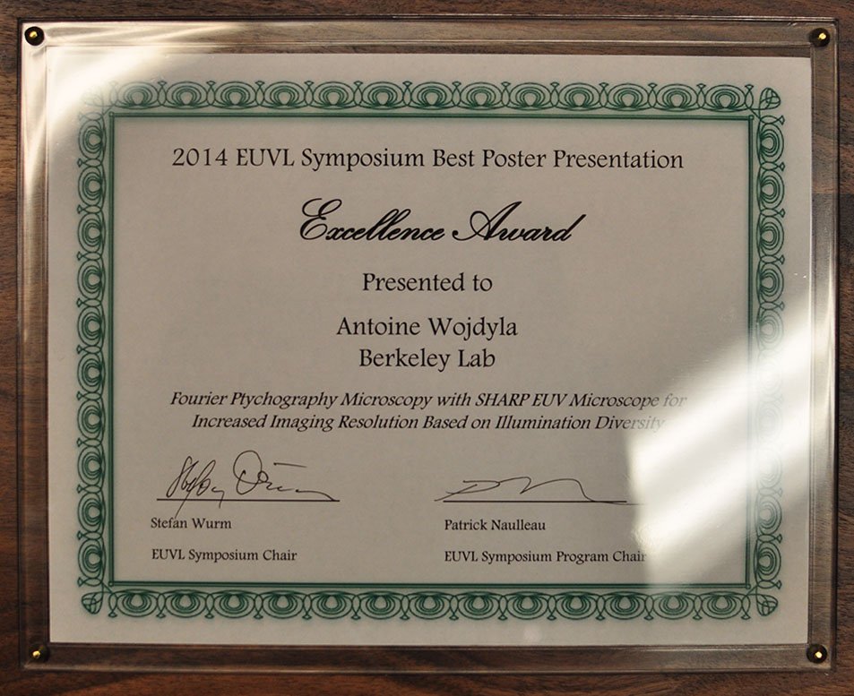
Award from the EUV Lithography Symposium :)
There are also other advantages that are related to the use of a lens with a smaller numerical aperture.
First, the field of view (which varies as 1/NA) gets much bigger, so that the compound information in your image gets much bigger : thanks to the increased space-bandwidth product, you can have, in some cases, gigapixels images.
Also, the depth of focus (which varies as 1/NA^2) is way bigger too : you can have in your image a bigger volume “in-focus”, hence even more information.